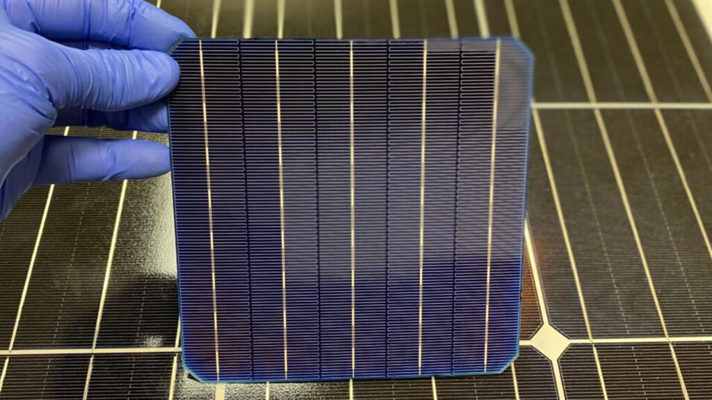
Process: texturing (INTEX)→diffusion (DIFF)→post-cleaning (cutting/removing PSG)→anti-reflection coating (PECVD)→screening, sintering (PRINTER)→testing, sorting (TESTER+SORTER)→packaging (PACKING)
1.PV panel Cell texturing
The purpose of texturing is to form a textured surface on the surface of the silicon wafer to reduce the reflectivity of the cell. The unevenness of the textured surface can increase secondary reflection and change the optical path and incident mode.
Usually, single crystals are treated with alkali to obtain pyramid-shaped suede; poly crystals are treated with acid to obtain wormhole-shaped random suede. The difference in processing methods is mainly in to the nature of single polycrystalline
Technological process: cashmere tank→water washing→water washing→acid washing→water washing→drying.
In general, silicon is considered non-reactive with HF and HNO3 (silicon surface will be passivated). When present in the system of two mixed acids, the reaction of silicon with the mixed solution is continuous.
2. Diffusion of PV panelcells
Diffusion is to make the heart of the battery, and it is to make the P-N junction for the battery. POCl3 is the current choice for phosphorus diffusion. POCl3 is a liquid phosphorus source, and the diffusion of the liquid phosphorus source has the advantages of high production efficiency, good stability, a uniform and smooth PN junction, and a good surface of the diffusion layer.
POCl3 breaks down at temperatures above 600°C to create phosphorus pentachloride (PCl5) and phosphorus pentoxide (P2O5). PCl5 is harmful to the surface of silicon wafers. In the presence of oxygen (O2), PCl5 decomposes into P2O5 and releases chlorine gas. Therefore, a controlled flow of oxygen is introduced while nitrogen is dispersed.
At the diffusion temperature, P2O5 reacts with silicon to produce silicon dioxide (SiO2) and phosphorus atoms. The resulting P2O5 is deposited on the silicon wafer’s surface and continues to react with silicon, forming additional SiO2 and phosphorus atoms. This process leads to the formation of phosphorus-silicate glass (PSG) on the silicon wafer’s surface.
Phosphorus atoms diffuse into silicon, resulting in the creation of an N-type semiconductor.
3. Etching of PV panel cells
During the diffusion process, the back-to-back single-sided diffusion method is used, leading to the diffusion of phosphorus atoms on the side and back edges of the silicon wafer.
When sunlight is present, the electrons generated by light and collected on the front side of the P-N junction flow to the back side through the region where phosphorus is diffused along the edge, causing a short circuit.
Shorting the channel reduces the parallel resistance.
The etching process aims to remove the phosphorus portion on the edge of the silicon wafer to prevent a short circuit of the P-N junction and reduce the parallel resistance.
Wet etching process: film loading → etching tank (H2SO4 HNO3 HF) → water washing → alkali bath (KOH) → water washing → HF bath → water washing → film removal
HNO3 reacts and oxidizes to produce SiO2, while HF is used to remove SiO2. The alkali tank etching process serves to smoothen the untextured surface and make it uniform. The main solution used in the alkali tank is KOH. H2SO4 is used to facilitate the movement of silicon wafers on the assembly line and does not participate in the reaction.
Dry etching refers to thin film etching using plasma. When the gas is in the plasma state, it becomes more chemically active.
By choosing a suitable gas, the silicon wafer can react quickly and undergo etching. Additionally, the electric field is used to guide and accelerate the plasma, giving it energy. When the silicon wafer’s surface is bombarded, the atoms of the silicon material are dislodged, achieving etching through the transfer of physical energy.
4. PECVD
Plasma Chemical Vapor Deposition (PCVD) is a process used to deposit a thin film on the surface of silicon. When sunlight hits the silicon surface, about 35% of it gets reflected. To improve the absorption of sunlight by the solar cell, an anti-reflection film is applied. This film increases the photo-generated current, leading to higher conversion efficiency.
Additionally, the film containing hydrogen passivates the cell surface, reducing surface recombination at the emitter junction. This lowers the dark current, increases the open circuit voltage, and improves the overall photoelectric conversion efficiency. Hydrogen in the film can react with defects or impurities in the silicon. This reaction shifts energy from the forbidden band to the valence band or conduction band.
In a vacuum environment at a temperature of 480 degrees Celsius, a layer of SixNy film is applied to the surface of the silicon wafer using a graphite boat as a conductor.
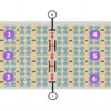
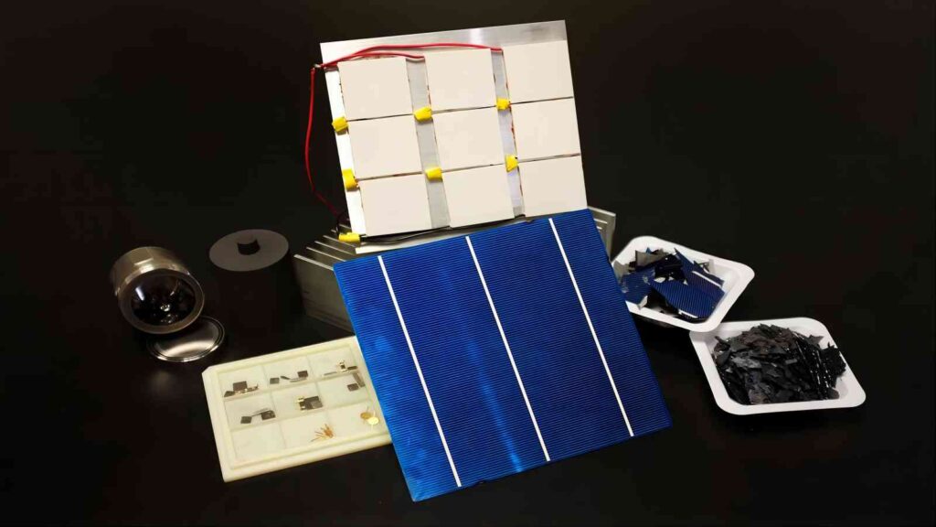
5. Screen printing of PV panel cells
In simple terms, the process involves collecting current and creating electrodes for solar cells. Firstly, a silver electrode is applied to the back of the cell, followed by printing and drying an aluminum back field. Then, a front silver electrode is printed, focusing on controlling the wet weight and width of the sub-grid.
If the wet weight of the second step is too high, it leads to waste of the slurry and insufficient drying before entering the high-temperature zone. This can result in the organic matter remaining in the slurry, preventing the complete transformation into metal aluminum.
Excessive weight can also cause the solar cell to become curved after sintering. If the wet weight is too low, all the aluminum paste is consumed during sintering. This forms an alloy area with silicon that is not suitable for back metal contact. This is because lateral conductivity and solderability are poor. Additionally, it may cause bulges or other appearance defects.
If the width of the third grid line is too wide, it reduces the light-receiving area of the cell and decreases efficiency.
Printing method: physical printing, drying
6. Sintering of PV panel cells
Sintering is the process of heating the electrode printed on the cell’s surface at a high temperature. This helps the electrode and the silicon chip form good electrical contact, improving the cell’s open circuit voltage and fill factor. It also ensures that the electrode has low resistance, leading to high conversion efficiency.
Sintering helps facilitate the diffusion of hydrogen into the PECVD process. This effective passivation of the cell is an added benefit.
The sintering method used is high temperature rapid sintering, and the heating is achieved through infrared heating.
Sintering is a comprehensive process of diffusion, flow, and physical and chemical reactions. The front Ag diffuses into the silicon through SiNH but cannot reach the P-N surface, and the back Ag and Al diffuse into the silicon. Due to the need to form an alloy, a certain temperature is required. Ag, The stability of alloys formed by Al and Si is different, so it is necessary to set different temperatures to achieve alloying, respectively.
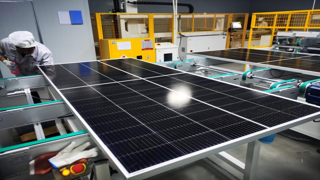
Since 2008, Mosaic Solar has been focusing on the production of various photovoltaic modules, and we provide a series of glass modules using PERC technology for you to choose.
Why Do Solar Panels Lose Power in Hot Weather? How Temperature Coefficient and Roof Ventilation Affect Summer Energy Yield
Summer brings stronger sunlight and longer daylight hours, so it is normally one of the most productive seasons for a solar system. However, some system owners notice that solar panel output does not continue to rise during the hottest part of the day.
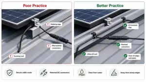
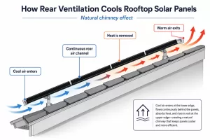
How to Design a Low-Maintenance Rooftop Solar System
Introduction A low-maintenance rooftop solar system is not created after installation. It is designed before installation. Over a 20–30 year operating life, rising O&M costs are rarely caused by dirty glass alone. They are more often caused by design decisions made at the
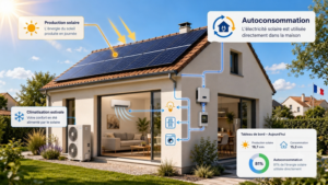
European Heatwaves and PV Self-Consumption: Why HJT Solar Modules Perform Better in Hot Summers
Across Europe, summer heatwaves are no longer just a climate or comfort issue. They are becoming an energy-use issue. During hot summer days, air conditioning, ventilation, refrigeration, office equipment and industrial cooling loads can rise exactly when rooftop solar modules are exposed to
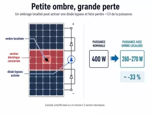
Partial Shading on Solar Panels: Why a Small Shadow Can Cause Major Power Losses
Introduction: Shading Is Not Just a Surface Area Problem In a photovoltaic system, a small shadow can be amplified by the electrical structure of the module. In a typical module with three electrical sections, a shaded area covering only a small part of
From Half-Cell to Multi-Cut: Why PV Modules Are Paying More Attention to More Segmented Circuit Design?
Table of Contents In recent years, half-cell modules have become a mainstream design in the photovoltaic market. Compared with traditional full-cell modules, half-cell technology reduces the operating current of each cell unit, lowers internal resistive losses, and improves thermal management and partial shading
Does Summer Heat Reduce Solar Panel Efficiency? What Really Happens to PV Output
Table of Contents Many PV users notice an unusual phenomenon in summer: although sunlight is strongest at noon, the power curve shown in the monitoring app does not reach the expected peak. In contrast, on a sunny spring day, or just after a